DisEnchantment
Golden Member
Speculate at will
Last edited:
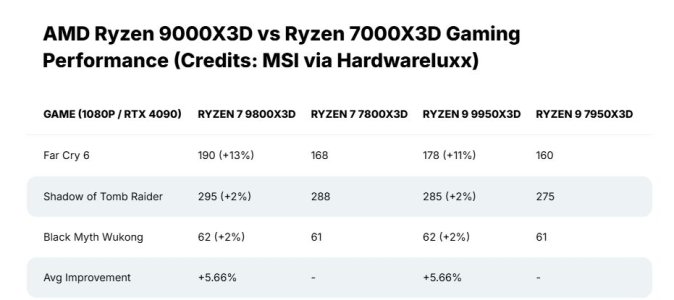
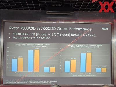
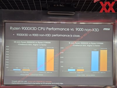
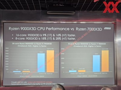
That's like a two weeks old 'leak' by MSI, and they've tested Wukong and SOTTR in 4K or something like thatCould these be legit?
Why in quotes?That's like a two weeks old 'leak' by MSI, and they've tested Wukong and SOTTR in 4K or something like that

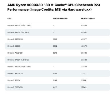
 browser.geekbench.com
It’s these slides from a larger presentation that hardwareluxx attended and for some reason photographed (despite nda language on the literal slides they photographed) at msi offices and then briefly published on their website before removing. There’s errors in the slides (discrepancies between titles and legends), only 3 games tested, and very little transparency into testing conditions, so make of them what you will. ‘Leak’ in the sense that they were intentionally presented by MSI to press but not intended for wider consumption.Why in quotes?
Ah... gotcha, so it was intentional... )‘Leak’ in the sense that they were intentionally presented by MSI to press but not intended for wider consumption.
Did you set MEM VPP at 1.35 manually or is it by the board's auto? I am seeing 1.80 when left auto. As a matter of fact I do not even remember I've seen that option in the BIOS.sure
before (EXPO enabled, all timmings auto):
View attachment 110282
After (EXPO enabled, all timmings auto):
View attachment 110283
So as @tsamolotoff said, it sets tREFI to a higher value and tRFC to a lower value.. and thats it
btw @Hitman928, I set "EXPO/XMP high bandwidth support" to disabled, and it was not enabled after enabling this x3d turbo mode thing (and restarting) 🧐
Pretty old "news" at this point if you have been following this thread 😉
Pretty old "news" at this point if you have been following this thread 😉
AMD is cheap. Don't you know? 🙂BTW, if it is true and L3 die is below, then why not make SRAM amount > 64 MB? There would be room for more on the die.
AMD is cheap. Don't you know? 🙂
Does it matter if they crush the competition 20% or 30% in gaming ? (and they kinda want to keep the die hight the same)BTW, if it is true and L3 die is below, then why not make SRAM amount > 64 MB? There would be room for more on the die.
I am hoping that 12 and 16C X3D will have higher clock 3D chiplet clocks. That would be incentive to some potential buyers to opt for higher core count X3D parts, especially if they will have higher OC ceiling on the 3D chiplet.Does it matter if they crush the competition 20% or 30% in gaming ? (and they kinda want to keep the die hight the same)
Think this is also the reason for the conservative clocks on the first SKU.. It will be up to us tinkers to push the silicon and really show what it can do 🙂
Does it matter if they crush the competition 20% or 30% in gaming ? (and they kinda want to keep the die hight the same)
Think this is also the reason for the conservative clocks on the first SKU.. It will be up to us tinkers to push the silicon and really show what it can do 🙂
More 3D cache isn't going to help in clone markets. It's already the biggest stick. They need to crack the volume markets in OEMs and corporate and you don't do that with a low volume part (that you can't make in high volumes). Especially by making the production even lower volume by adding two stacks.It does matter. It took very large performance delta for AMD to make inroads to datacenter (with chiplets), and it may take similar delta to make similar inroads in client markets.
As far as height, I was still thinking single layer, but instead of die area of 1/2 of CCD, using same die size for V-Cache as main CCD. Which should fit ~128 MB.
Yeah, it does seem like very conservative clock speed, if there isn't any inherent limiting factor, compared to standard Zen 5 CPUs. Maybe 9850x3d mid-way between Zen 5 and Zen 6 releases.
It's a Zen Timmings misread. It seems VDDQ and VPP values are exchangedDid you set MEM VPP at 1.35 manually or is it by the board's auto? I am seeing 1.80 when left auto. As a matter of fact I do not even remember I've seen that option in the BIOS.
Press only event to cover the launch?https://pbs.twimg.com/media/GaLTfYuagAAeh37?format=jpg&name=large
If there's no announcement being made then what is this invitation letter for??
I thought the cache on previous versions meant you can get away with lower bandwidth before. An understated part of the value prop for them.With X3D it seems like there is even more reason to push higher memory bandwidth than ever.
High price 😂Well AMD did hint that the 2 CCD V cache parts were “special” no?
What else could make them special?
BTW, if it is true and L3 die is below, then why not make SRAM amount > 64 MB? There would be room for more on the die.